
Nanoscience
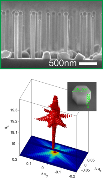
Semiconductor NanowiresSemiconductor nanowires (NWs) are promising candidates for the fabrication of future electronic or optoelectronic devices and have attracted increasing interest in recent years. Amongst others, possible applications range from light emitting diodes and NW lasers, over photovoltaic applications in solar cells to electronic devices like field effect transistors or even sensors for gases or proteins. Using different growth techniques, it is possible to grow a large variety of nanowires on different substrates. However, many fundamental aspects of nanowire growth are not fully understood, and major drawbacks remain to be solved. X-ray diffraction provides a valuable tool to study the structure and possible strains in NWs with high accuracy. Conventional x-ray diffraction techniques employ x-ray beams with typical dimensions of 100µm and allow to study large ensembles of NWs simultaneously. In addition, we use the capabilities of modern x-ray optics to focus x-ray beams at synchrotron sources to sizes in the nanometer regime and to perform high resolution diffraction experiments on single NWs. Because even NWs grown simultaneously next to each other can differ in their individual structure, this method allows to measure and compare individual properties. Recent publications:
|  | |||
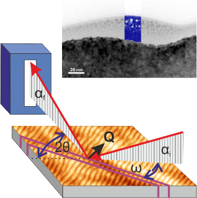
Ion-beam induced nanostructures on siliconIon-beam sputtering of semiconductor surfaces allows the fabrication self-organized nanostructures on large surface areas in a short time. For example, the oblique bombardment of silicon surfaces with energetic noble-gas ions can produce well-ordered ripple patterns with typical wavelengths in the range of 10s to 100s of nanometers. However, many parameters influencing the pattern formation are not finally understood. For example, pattern formation frequently occurs only in the presence of metallic adatoms on the surface. Furthermore, the bombardment of the crystal lattice with energetic ions leads to the formation of defects and a partial amorphization of the material, whose role is not fully understood. Using surface sensitive x-ray techniques like x-ray reflectivity or grazing incidence diffraction, we study the influence of ion implantation on the morphology and crystal structure of the silicon substrate. Further reading:
|  | |||