
Research
Outreach
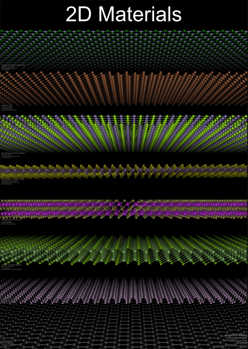
Our research is centered around 2D materials. You can find the image below with enough resolution to be printed as a poster here. Contact us in case you are interested in the source file.
2D-InTune (Tuning the electronic structure of two-dimensional semiconductor junctions)
Funding: European Commission through Horizon Europe Framework Programme
Start: 07/2023
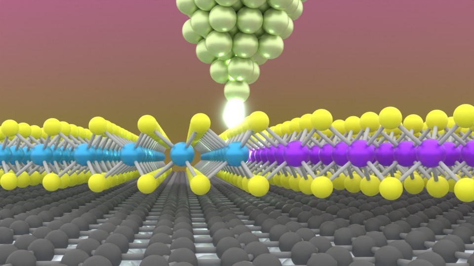
Semiconductor junctions composed of 2D transition metal dichalcogenides (TMDs) will be prepared on hexagonal boron nitride (hBN) or graphene (Gr) on Ir(111). The use of the single-crystalline metal substrate allows the application of surface science methods for preparation and characterization, while the ultrathin buffer layer leaves the intrinsic properties of TMDs undisturbed. Intercalation of guest atoms between the buffer layer and Ir will be used as an elegant and non-invasive method for doping the TMDs. This will also tune intrinsic band bending at the 1D-interface of the TMD junctions, which is yet to be explored for various 2D systems.
To separate the effect of inhomogeneous doping and inhomogeneous structure, two types of lateral TMD junctions will be prepared: Homojunctions will be achieved by doping only one part of the TMD island by extending it over the interface of intercalated patches in hBN. Heterojunctions will be composed of two different TMD materials grown on homogeneous vdW substrate, either fully intercalated or pristine. Samples will be prepared by combining two TMDs (ReS2 and WS2) and two dopants (n and p). Scanning tunneling spectroscopy (STS) and Kelvin probe force microscopy (KPFM) will be used for the characterization of the 1D-interfaces and the reconstruction of the band diagrams. Dielectric screening induced by the substrate will be analyzed by comparing values of the band gaps and shifts of critical energy points between different systems. This will deepen the understanding of the origin of band bending in 2D systems. Inelastic electron tunneling spectroscopy (IETS) will be used as a potentially new technique for detecting excitons.
Two-dimensional ferroelectrics
Funding: German Science Foundation (DFG)
Start: 01/22
Ferroelectric materials are a recent addition to the two-dimensional world with fascinating fun-damental properties as well as a high potential for applications. In analogy to ferromagnets, ferroelectrics show a permanent electrical polarization that can be switched by an external electric field. The reduced dimensionality in ultrathin layers as well as competing modes of coupling in van der Waals stacks induce novel effects in 2D-ferroelectrics.
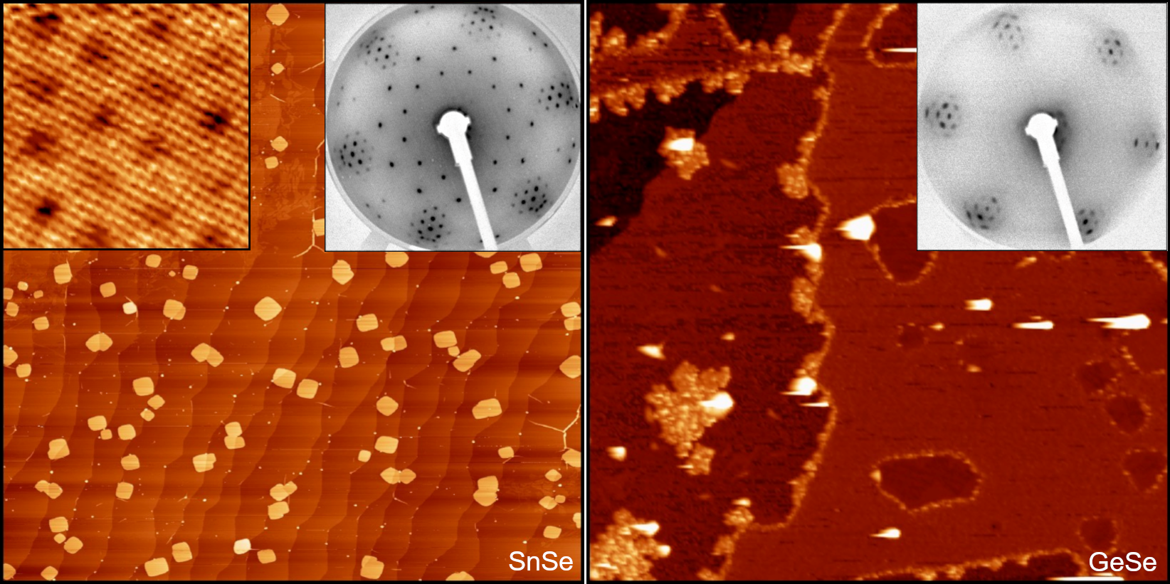
In thin films of conventional ferroelectrics, the critical temperature TC decreases with decreas-ing thickness and quickly drops below feasible values. In contrast, in two-dimensional group-IV monochalcogenides, very stable (in-plane) ferroelectricity is found. These materials of the form MX (M=Ge, Sn; X=S, Se, Te) are in the focus of this project. Here, ferroelectricity arises from the loss of centrosymmetry in the puckered crystal structure in combination with the ionic character of the bonds.
The samples in this project will be prepared by epitaxial growth under highly-controlled condi-tions (well-defined substrate, UHV environment) which is a versatile method to prepare ad-vanced 2D materials, in this case quasi-freestanding mono- as well as few-layered MX. Our main methods for sample characterization are scanning tunneling microscopy (STM) and scanning tunneling spectroscopy (STS).
We will investigate the switching of the polarization by applying a point-like electric field using the STM tip and by exploiting the auxetic behavior of MX and apply a vertical strain with the AFM which induces a compression in-plane, moving the system towards the saddle point of the switching. A switchable polarization of this kind would also be interesting from the view-point of applications. On a more fundamental scale, in the MX also a ferroelastic switching is possible, which corresponds to a rotation by 90°.
The interaction between neighboring layers in van der Waals-stacks is decisive for the ferroe-lectricity: The in-plane dipoles prefer an antiferroelectric coupling (AB-stacking), while the local ionic and covalent coupling prefers an AA stacking with ferroelectric coupling. The resulting interaction energies have different dependencies on the number of layers, and hence the pre-ferred stacking can change with film thickness. For the specific case of GeSe, AA stacking is the energetic minimum for the bilayer, but AB stacking is preferred in the bulk. We will investi-gate this interplay of local and non-local coupling in different MX (GeSe, GeS, SnSe, SnS) to pin down the influence of the individual constituents. In such a system, switching of one layer only would lead to a moiré-structure between two ferroelectric layers, which is a completely unexplored system.
Phase engineering in transition metal dichalcogenides
Funding: Alexander von Humboldt Foundation
Start: 01/22
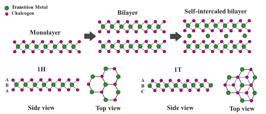
We investigate transition metal dichalcogenides, exploring different experimental routes to trigger phase transition, favoring the formation of metastable phases with unique properties. The methodologies to achieve this goal are: molecular-beam epitaxy under highly controlled conditions, intercalation of specific species, inclusion of substitutional atoms, ion irradiation and the synthesis of multilayer systems. To investigate such systems scanning tunneling microscopy and spectroscopy is employed, which allows the distinction of different phases within the same sample and the study of how their structural and electronic properties vary under specific conditions.